- 您现在的位置:买卖IC网 > Sheet目录2009 > MAX1499ECJ+ (Maxim Integrated Products)IC ADC 3 1/2DIG W/LED DVR 32TQFP
MAX1497/MAX1499
3.5- and 4.5-Digit, Single-Chip ADCs with LED
Drivers and C Interface
10
______________________________________________________________________________________
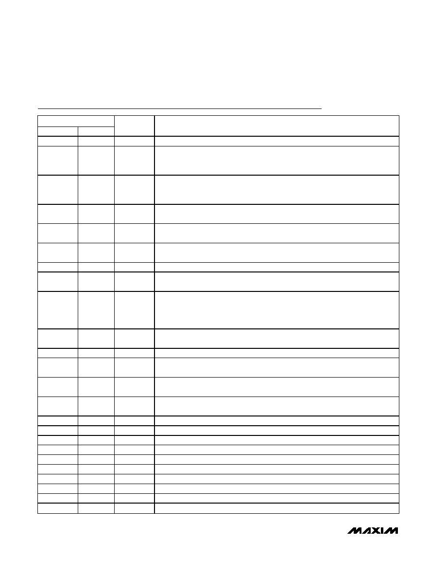
Pin Description
PIN
MAX1497
MAX1499
NAME
FUNCTION
131
VNEG
-2.5V Charge-Pump Voltage-Output. Connect a 0.1F capacitor to GND.
232
REF-
Negative Reference Voltage Input. For internal reference operation, connect REF- to
GND. For external reference operation, bypass REF- to GND with a 0.1F capacitor and
set VREF- from -2.2V to +2.2V, provided VREF+ > VREF-.
31
REF+
Positive Reference Voltage Input. For internal reference operation, connect a 4.7F
capacitor from REF+ to GND. For external reference operation, bypass REF+ to GND
with a 0.1F capacitor and set VREF+ from -2.2V to +2.2V, provided VREF+ > VREF-.
42
AIN+
Positive Analog Input. Positive side of fully differential analog input. Bypass AIN+ to GND
with a 0.1F or greater capacitor.
53
AIN-
Negative Analog Input. Negative side of fully differential analog input. Bypass AIN- to
GND with a 0.1F or greater capacitor.
64
ISET
Segment Current Controller. Connect to ground through a resistor to set the segment
current. See Table 6 for segment current selection.
75
GND
Ground
8—
VDD
Analog and Digital Circuit Supply Voltage. Connect VDD to a +2.7V to +5.25V power
supply. Bypass VDD to GND with a 0.1F and a 4.7F capacitor.
98
CLK
External Clock Input. When the EXTCLK register bit is set to one, CLK is the master clock
input (frequency = 4.9152MHz) for the modulator and the filter. When the EXTCLK
register bit is reset to zero, the internal clock is used. Connect CLK to GND or DVDD
(MAX1499) or VDD (MAX1497) when the internal oscillator is used.
10
9
EOC
Active-Low End-of-Conversion Logic Output. A logic low at EOC indicates that a new
ADC result is available in the ADC result register.
11
10
CS
Active-Low Chip Select Input. Forcing CS low activates the serial interface.
12
11
DIN
Serial Data Input. Data present at DIN is shifted into the internal registers in response to
a rising edge at SCLK when CS is low.
13
12
SCLK
Serial Clock Input. Apply an external clock to SCLK to facilitate communication through
the serial bus. SCLK may idle high or low.
14
13
DOUT
Serial Data Output. DOUT presets serial data in response to register queries. Data shifts
out on the falling edge of SCLK. DOUT goes high impedance when CS is high.
15
14
DIG0
Digit 0 Driver
16
15
DIG1
Digit 1 Driver
17
16
GLED
Ground for LED-Display Segment Driver
18
17
DIG2
Digit 2 Driver
19
18
DIG3
Digit 3 Driver
20
SEGA
Segment A Driver
21
SEGB
Segment B Driver
22
SEGC
Segment C Driver
23
SEGD
Segment D Driver
24
SEGE
Segment E Driver
发布紧急采购,3分钟左右您将得到回复。
相关PDF资料
MAX152EPP+
IC ADC 8BIT 1UA PWR-DWN 20-DIP
MAX153EPP+
IC ADC 8BIT 1MSPS HI-SPD 20-DIP
MAX154AENG+
IC ADC 8BIT 4CH W/MUX&REF 24-DIP
MAX155AEPI+
IC ADC 8BIT 8CH T/H&REF 28-DIP
MAX157AEUA+
IC ADC 10BIT 108KSPS 2CH 8-UMAX
MAX160CPN+
IC ADC 8BIT UP COMPATIBLE 18-DIP
MAX165ACPN+
IC ADC CMOS 8BIT UP COMP 18-DIP
MAX170CEPA+
IC ADC 12BIT SERIAL 8-DIP
相关代理商/技术参数
MAX1499ECJ+T
功能描述:模数转换器 - ADC 4.5 Digit ADC w/LED Drivers RoHS:否 制造商:Texas Instruments 通道数量:2 结构:Sigma-Delta 转换速率:125 SPs to 8 KSPs 分辨率:24 bit 输入类型:Differential 信噪比:107 dB 接口类型:SPI 工作电源电压:1.7 V to 3.6 V, 2.7 V to 5.25 V 最大工作温度:+ 85 C 安装风格:SMD/SMT 封装 / 箱体:VQFN-32
MAX1499ECJ-T
功能描述:模数转换器 - ADC RoHS:否 制造商:Texas Instruments 通道数量:2 结构:Sigma-Delta 转换速率:125 SPs to 8 KSPs 分辨率:24 bit 输入类型:Differential 信噪比:107 dB 接口类型:SPI 工作电源电压:1.7 V to 3.6 V, 2.7 V to 5.25 V 最大工作温度:+ 85 C 安装风格:SMD/SMT 封装 / 箱体:VQFN-32
MAX1499EVC16
功能描述:模数转换器 - ADC 3.5- and 4.5-Digit Single-Chip ADCs with LED Drivers and uC Interface RoHS:否 制造商:Texas Instruments 通道数量:2 结构:Sigma-Delta 转换速率:125 SPs to 8 KSPs 分辨率:24 bit 输入类型:Differential 信噪比:107 dB 接口类型:SPI 工作电源电压:1.7 V to 3.6 V, 2.7 V to 5.25 V 最大工作温度:+ 85 C 安装风格:SMD/SMT 封装 / 箱体:VQFN-32
MAX1499EVKIT
功能描述:数据转换 IC 开发工具 Evaluation Kit/Evaluation System for the MAX1499 RoHS:否 制造商:Texas Instruments 产品:Demonstration Kits 类型:ADC 工具用于评估:ADS130E08 接口类型:SPI 工作电源电压:- 6 V to + 6 V
MAX149ACAP
功能描述:模数转换器 - ADC Integrated Circuits (ICs) RoHS:否 制造商:Texas Instruments 通道数量:2 结构:Sigma-Delta 转换速率:125 SPs to 8 KSPs 分辨率:24 bit 输入类型:Differential 信噪比:107 dB 接口类型:SPI 工作电源电压:1.7 V to 3.6 V, 2.7 V to 5.25 V 最大工作温度:+ 85 C 安装风格:SMD/SMT 封装 / 箱体:VQFN-32
MAX149ACAP+
功能描述:模数转换器 - ADC 10-Bit 8Ch 133ksps 5.25V Precision ADC RoHS:否 制造商:Texas Instruments 通道数量:2 结构:Sigma-Delta 转换速率:125 SPs to 8 KSPs 分辨率:24 bit 输入类型:Differential 信噪比:107 dB 接口类型:SPI 工作电源电压:1.7 V to 3.6 V, 2.7 V to 5.25 V 最大工作温度:+ 85 C 安装风格:SMD/SMT 封装 / 箱体:VQFN-32
MAX149ACAP+T
功能描述:模数转换器 - ADC 10-Bit 8Ch 133ksps 5.25V Precision ADC RoHS:否 制造商:Texas Instruments 通道数量:2 结构:Sigma-Delta 转换速率:125 SPs to 8 KSPs 分辨率:24 bit 输入类型:Differential 信噪比:107 dB 接口类型:SPI 工作电源电压:1.7 V to 3.6 V, 2.7 V to 5.25 V 最大工作温度:+ 85 C 安装风格:SMD/SMT 封装 / 箱体:VQFN-32
MAX149ACAP-T
功能描述:模数转换器 - ADC RoHS:否 制造商:Texas Instruments 通道数量:2 结构:Sigma-Delta 转换速率:125 SPs to 8 KSPs 分辨率:24 bit 输入类型:Differential 信噪比:107 dB 接口类型:SPI 工作电源电压:1.7 V to 3.6 V, 2.7 V to 5.25 V 最大工作温度:+ 85 C 安装风格:SMD/SMT 封装 / 箱体:VQFN-32